Premier Patent Attorney with a Personal Touch
With over 27 years of dedicated service as a patent attorney, I bring a wealth of experience from my private practice and my time as in-house corporate counsel at Texas Instruments Inc. My time in the intellectual property landscape has been deeply intertwined with the world of semiconductor design and process, digital and analog design, and the ever-evolving field of wireless technology.
As an intellectual property attorney with a unique background in engineering, I understand the intricacies of the legal and technical aspects of patent law. As a trademark attorney in various licensing roles, I’ve prepared and presented persuasive claim charts, facilitated Patent Proud List preparations, and steered licensing offenses and defenses with strategic insight.
My 15 years as a design engineer and Senior Member of the Technical Staff at Texas Instruments have given me a practical understanding that betters my approach to semiconductor patents. Connect with me on LinkedIn to learn more.
Patent Attorney at Your Service
My specific focus as a semiconductor patent attorney is informed by my engineering experience, allowing me to navigate the complex technical details crucial to semiconductor inventions. This unique expertise ensures that your intellectual property is protected with the depth of understanding it deserves.
Rooted in Discipline and a Passion for Balance
I am a former U.S. Army Officer and was granted a military leave of absence by Texas Instruments Inc. My service spanned from 1977 until my honorable discharge in 1985, during which I embraced and completed various development courses. My military education included the Infantry Officer Basic and Advanced courses, Airborne and Ranger training, and Army Trainer Development Program participation.
These military experiences instilled a profound sense of discipline, strategic thinking, and resilience, influencing my approach to intellectual property law and enriching my client advocacy.
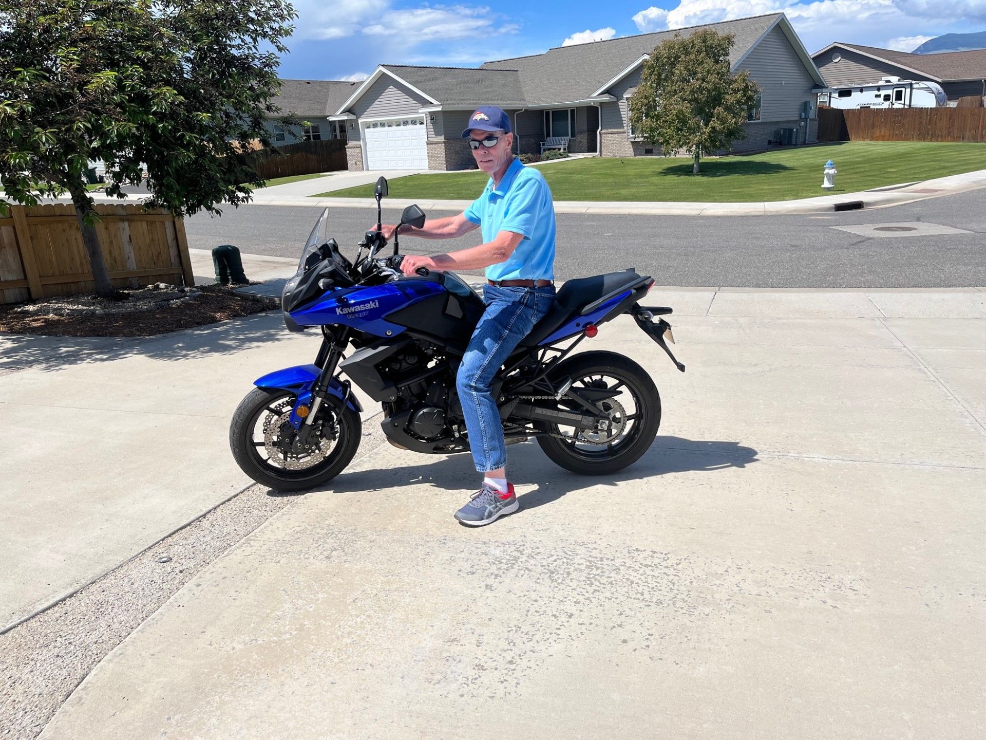
When I step away from the legal documents, I find solace in cycling and gardening – interests that keep me connected to life’s simple pleasures and provide a counterbalance to the rigors of legal practice.
Mission
As a Patent Attorney, inventor, and former design engineer, I understand the importance of intellectual property protection from corporate and individual perspectives. I will help others understand relevant aspects of Patent and Trademark law and help them make sound decisions regarding their intellectual property. I will ensure clients see all communication from the United States Patent and Trademark Office, and I will explain and seek approval for all my responses.
Contact
Reach out today, and let’s make sure your innovations are protected and your vision is realized.
Robert N. Rountree
robert@rountreeip.com
3419 Appalachian Ave.
Cody, WY 82414
LinkedIn: https://www.linkedin.com/in/robert-rountree-a3bb51265/
Education:
1996 JD, Texas Wesleyan School of Law, Fort Worth, TX
1976 BSEE, University of Houston, Houston, TX
Bar Admissions:
1997 State of Texas (00798475)
1995 US Patent & Trademark Office (39,347)
Experience:
- Expert witness for Samsung Electronics Co., Ltd. v. Matsushita Electric Industrial Co.., Ltd. et al., 6:06-CV-154 (E.D. Tex.).
- Expert witness for Infineon Technologies North America Corp. (P) v. Mosaid Technologies, Inc. (D) and Mosaid Technologies Inc. (CC) v. Infineon Technologies North America Corp., Infineon Technologies AG, Infineon Technologies Holding North America Inc., and Infineon Technologies Richmond LP, (CD) 03-CV-4698.
- Expert witness for Mosaid Technologies Inc. (P) v. Infineon Technologies North America Corp., Infineon Technologies AG, Infineon Technologies Holding North America Inc., and Infineon Technologies Richmond LP, (D) 6:05-CV-120.
- Expert witness for ST Microelectronics, Inc. (P) v. Sandisk Corp. (D) 4:05-CV-45.
- Patent prosecution and consulting from 2003 to present. Includes preparation and prosecution of patent applications, reexaminations, and reissues. Consulting includes licensing discussions, portfolio review, and validity and infringement issues.
- In charge of Semiconductor Licensing offense at Texas Instruments Inc. until 2003. Seven years plus experience with TI patent portfolio, analysis and selection of semiconductor patents for licensing, consultant interaction for claim chart production, claim chart presentation to licensees.
- Licensing experience includes preparation, presentation and argument of TI offensive patent infringement evidence before numerous U.S., Japanese, Korean, and Taiwanese companies. Experience in preparation and presentation of TI defense including consultant interaction, litigation support and validity searches.
- Prosecution experience includes working closely with technical community for patent disclosure acquisition, conducting TI memory patent committee meetings for selection and filing of key disclosures, writing and prosecution of patent applications, and requesting and prosecuting reexaminations of key TI patents.
- Litigation experience includes work with outside counsel, trial preparation, depositions, expert witness interaction, Markman hearings, and preparation of validity and infringement positions.
- Eleven years design experience including design on every generation of TI DRAM from 64 k through 64 M. Lead engineer on TI third generation 4 M DRAM. Design engineer on TI prototype 64 M DRAM responsible for column path and I/O path. Senior Member of Technical Staff 1987.
- EOS/ ESD circuit design and evaluation of TI ESD protection circuits for numerous technologies including DRAM, Nonvolatile, and Microprocessor. Evaluated numerous competitor ESD designs. Wrote ESD Design Guidelines used by most of TI for NMOS and CMOS process technologies.
- Work with EOS/ESD Symposium includes:
- EOS/ESD Symposium Moderator 1986-1987.
- EOS/ESD Design Workshop Panel Member 1987-1989.
- EOS/ESD Symposium Moderator 1986-1987.
- EOS/ESD Symposium Annual Best Paper and Best Presentation Awards 1988.
- EOS/ESD Steering Committee 1988-1989.
- EOS/ESD Technical Program Committee Member 1986-1989.
- EOS/ESD Technical Program Chairman 1989.
- Received Annual Outstanding Contribution Award and Lifetime Membership in EOS/ESD Association in 1989.
- Wrote and debugged Software Defect Analysis Expert System for DRAM defect analysis.
- Designed display logic and part of instruction decoder for TI-1500 Scientific calculator chip.
Patents:
- EP 0535536B1, Depletion controlled isolation stage 12/15/2001
- US 5,977,596, Depletion controlled isolation stage 11/2/1999
- US 5,925,922, Depletion controlled isolation stage 7/20/1999
- US 5,808,482, Row decoder with level translator 9/15/1998
- US 5,682,110, Low capacitance bus driver 10/28/1997
- US 5,668,485, Row decoder with level translator 9/16/1997
- US 5,576,633, Block specific spare circuit 11/19/1996
- US 5,548,225, Block specific spare circuit 8/20/1996
- US 5,424,977, Sense amplifier having shared dummy cell 6/13/1995
- US 5,394,370, High speed parallel test architecture 2/28/1995
- US 5,305,266, High speed parallel test architecture 4/19/1994
- US 5,291,437, Shared dummy cell 3/1/1994
- EP 0364186B1, Quasi-folded bitline 2/16/1994
- US 5,060,037, Output buffer with enhanced electrostatic discharge protection 10/22/1991
- US 5,034,920, Cross point array memory device 7/23/1991
- US 5,012,317, Electrostatic discharge protection circuit 4/30/1991
- US 4,939,616, Circuit structure with enhanced electrostatic discharge protection 7/3/1990
- US 4,855,620, Output buffer with improved ESD protection 8/8/1989
- US 4,692,781, Semiconductor device with electrostatic discharge protection 9/8/1987
- DE 69232257T2, Durch veramung kontrollierte isolationsstufe 1/17/2002
- JP 09172174A2, Semiconductor device 6/30/1997
- JP 07321318A2, Protection device for semiconductor device 12/8/1995
- JP 06196634A2, Depletion-controlled isolation stage 7/15/1994
- DE 68913126T2, Quasi-gefaltete bitleitung 5/26/1994
- JP 05089700A2, High speed parallel test mechanism 4/9/1993
- JP 04355960A2, Memory cell 12/9/1992
- JP 02223090A2, Pseudo folding bit line 9/5/1990
- JP 02058262A2, Electrostatic discharge-preventive diode for integrated circuit 2/27/1990
- JP 01020651A2, Semiconductor output buffer device 1/24/1989
- US 10,375,429, Audio System With Integral Hearing Test 8/6/2019
- US 10,848,877, Audio System With Integral Hearing Test 11/24/2020
Patents Sold to Taiwan Semiconductor in 2017:
- US 8,482,962, Low Noise Memory Array 7/9/2013
- US 8,477,526, Low Noise Memory Array 7/2/2013
- US 8,675,395 Low Noise Memory Array, 3/18/2014
- US 8,730,711 Low Noise Memory Array, 5/20/2014
- US 8,525,581, Power Supply Protection Circuit and Method 9/3/2013
- US 8,625,377, Low Voltage Efuse Programming Circuit and Method, 1/7/2014
- US 8,842,488, Low Voltage Efuse Programming Circuit and Method, 9/23/2014
- US 8,872,223, Programmable SCR for ESD Protection, 10/28/2014
- US 9,029,910, Programmable SCR for ESD Protection, 5/12/2015
- US 8,866,200, JFET ESD Protection Circuit for Low Voltage Applications, 10/21/2014
- US 9,035,363, JFET ESD Protection Circuit for Low Voltage Applications, 5/19/2015
- US 8,669,806, Low Voltage Antifuse Programming Circuit and Method, 3/11/2014
Publications:
- ESD Phenomena in Graded Junction Devices, 27th IRPS Proc., Apr. 1989.
- Internal Chip ESD Phenomena Beyond the Protection Circuit, IEEE Trans. ED, ED-35, Dec. 1988.
- A Process-Tolerant Input Protection Circuit for Advanced CMOS Processes, EOS/ESD Symp., Sept. 1988.
- Output ESD Protection Techniques for Advanced CMOS Processes, EOS/ESD Symp., Sept. 1988.
- Book Review of W.D. Greason, Electrostatic Damage in Electronics: Devices and Systems, IEEE Circuits and Devices, June 1988.
- Internal Chip ESD Phenomena Beyond the Protection Circuit, 26th IRPS Proc., Apr 1988.
- ESD Phenomena and Protection Issues in CMOS Output Buffers, 25th IRPS Proc., Apr. 1987.
- ESD Protection: Design and Layout Issues for VLSI Circuits, IEEE-IAS Proc., Oct. 1987.
- ESD Protection Reliability in 1μm CMOS Technologies, 24th IRPS Proc., Apr. 1986.
- ESD Protection Reliability in 1μm CMOS Technologies, TI Journal, Sept. 1986.
- Software Defect Analysis, TI Journal, AI Issue, 1986.
- Thick Oxide Device ESD Performance Under Process Variation, EOS/ESD Symp., Sept. 1986.
- Characterization of ESD Stress Testers, TI Journal, Sept. 1986.
- ESD Design Considerations for ULSI, EOS/ESD Symp., Sept. 1986.
- NMOS Protection Circuitry, IEEE Trans. ED, ED-32, May 1985.
- NMOS Protection Circuitry, TI Technical Report 03-84-17, July 1984.
- A Summary of Most Effective ESD Protection Circuits for MOS Memories and Their Observed Failure Modes, EOS/ESD Symp., Sept. 1983.
Employers:
- 4/23/2022 – Rountree Intellectual Property, LLC, Cody, WY
- 2002-2021 – Robert N. Rountree, LLC (LLC discontinued with move to WY)
- 2001-2002 – Texas Instruments, Dallas, TX, Senior Counsel
- 1997-2002 – Texas Instruments, Dallas, TX, Patent Licensing Counsel
- 1992-1996 – Texas Instruments, Dallas, TX, Patent Licensing Engineer
- 1986-1991 – Texas Instruments, Dallas, TX, Sr. Member Technical Staff
- 1982-1985 – Texas Instruments, Dallas, TX, Design Eng., DRAM Design
- 1978-1982 – U.S. Army, U.S. & Canal Zone, Infantry Officer
- 1976-1977 – Texas Instruments, Houston, TX, Design Engineer, TI Calculator Division
Memberships:
- Texas Bar Association
- IEEE
- EOS/ESD Association (Lifetime member)


